Laser Processing
Laser Processing
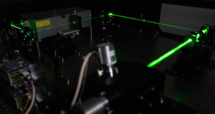
The precision machining by laser opens the door to new possibilities in the industry.
Laser processing has attracted widespread attention for its high precision and flexible characteristics , offering innovative possibilities for industry. We are researching methods to generate functional microstructures to influence the surface properties of materials using various laser processing.
3D microfabrication
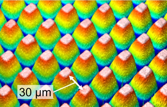
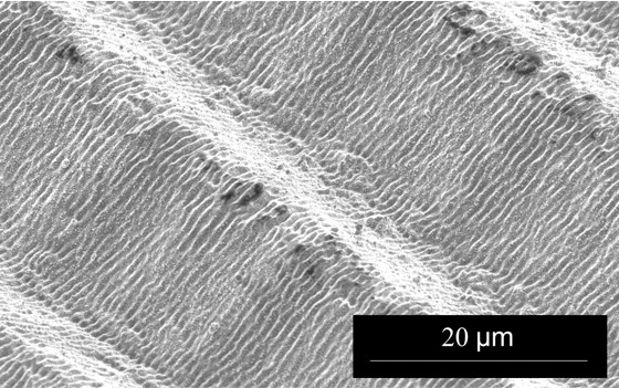
Scanning with ultrashort laser pulses enables high-precision processing with minimal thermal damage to the material and reduces burrs and cracks. We are attempting to create new surface functions by forming specific patterns of microscale holes, grooves, and nano-periodic surface microgroove structures on the surfaces of difficult-to-machine materials like single crystalline materials, ceramics, and hard brittle materials such as cemented carbides.
Laser repair of machining-affected layers
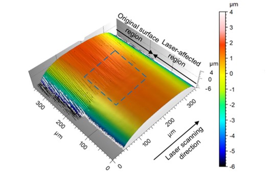
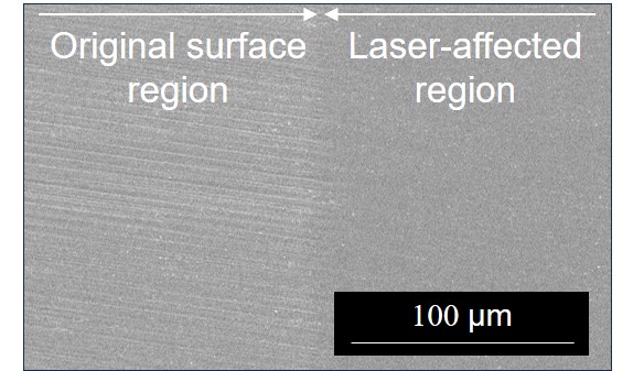
Even in nanoscale ultra-precision machining, a machining-affected layer inevitably forms on the surface of the workpiece. In our laboratory, we propose a laser repair technique that uses nanosecond pulsed laser irradiation to selectively melt only the machining-affected layer at a nanosecond scale. Subsequently, liquid-phase epitaxial crystal growth is initiated using the dislocation-free bulk region as a seed. This technique allows us to rapidly obtain a single-crystal surface to effected layer free and crack free surface.
Nanomaterial creation
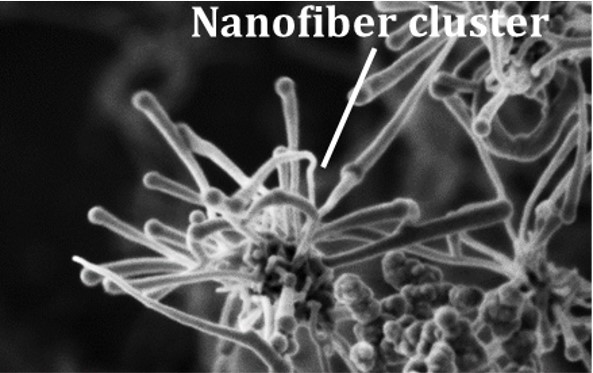
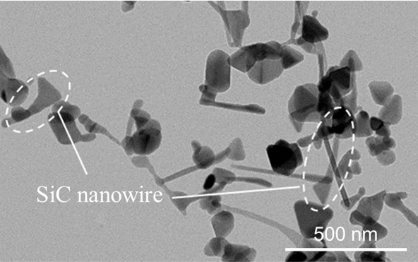
We are developing and evaluating nanocomposite materials with entirely new functionalities by binding and structurally controlling nanomaterials such as nanoparticles, nanofibers, nanotubes, and nanosheets using laser or infrared irradiation. For example, we have succeeded in developing high-capacity, long-life next-generation lithium-ion battery silicon anodes by forming nanoparticles through pulse laser irradiation of waste silicon powder generated in large quantities during the production processes of semiconductor devices and solar cells.
